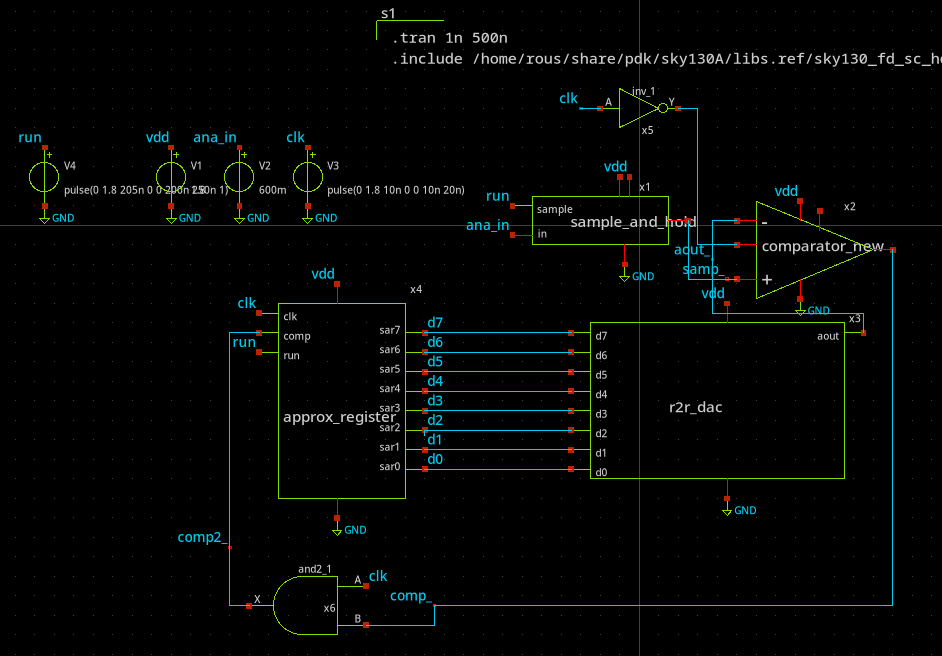
As a peripheral to the microcontroller, I designed an 8 bit successive approximation ADC. The main components are shown here, designed using the xschem schematic editor in separate sub-blocks, as well as the NGSpice testbench setup.

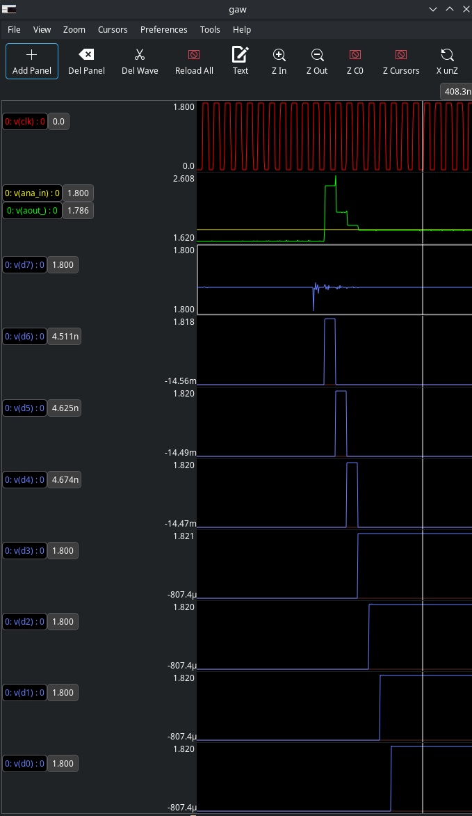
NGSpice simulations used SKY130 PDK SPICE models to make sure that timing and logic were correct. Here the ADC correctly digitizes 1.8V relative to a 3.3V supply.

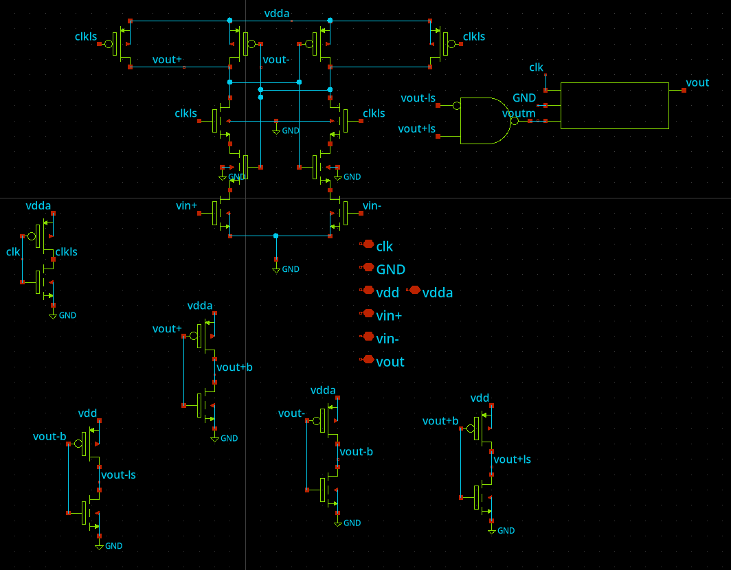
This clocked comparator included different MOSFET models and level shifters to account for the different voltage levels (3.3V analog domain, 1.8V digital domain)

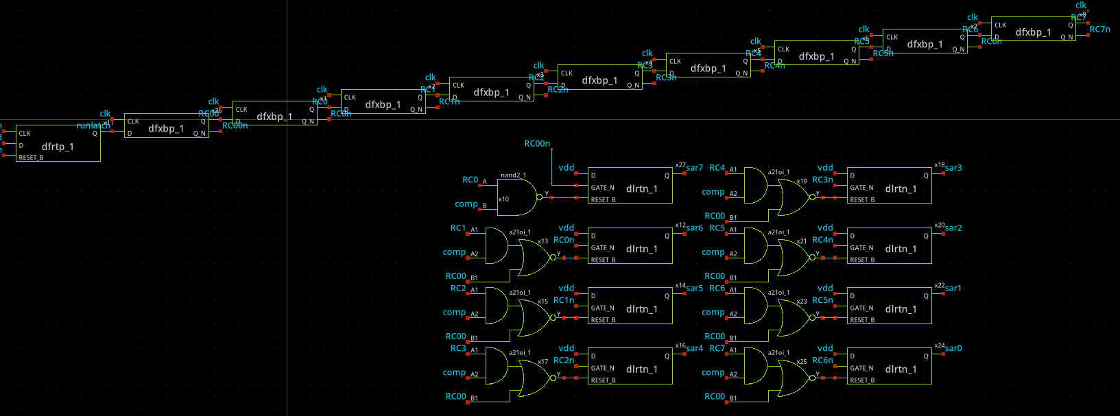
The successive approximation register was formed using SKY130 standard cell logic blocks to make layout easier.

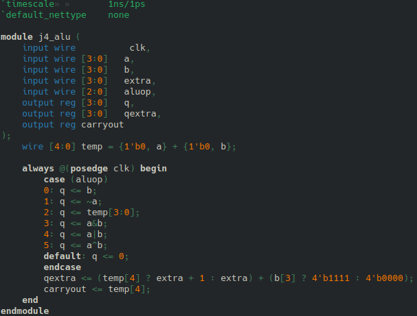
The digital block of the microcontroller was designed using verilog in multiple files. Here, the 4-bit ALU is displayed.

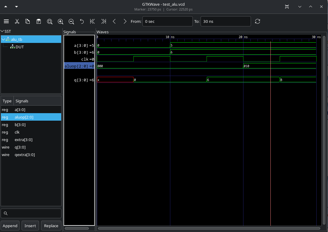
The digital components of the microcontroller were separately simulated using iverilog and GTKWave. I created test benches for each subcomponent to verify the designs separately.

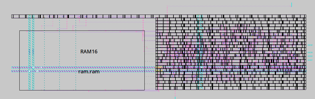
The librelane automated place-and-route software was used to generate the layout for digital blocks. The RAM16 block is an efficient D flip-flop RAM macro, Here, the CPU is shown, with power rails and a port for an SPI memory device (right).

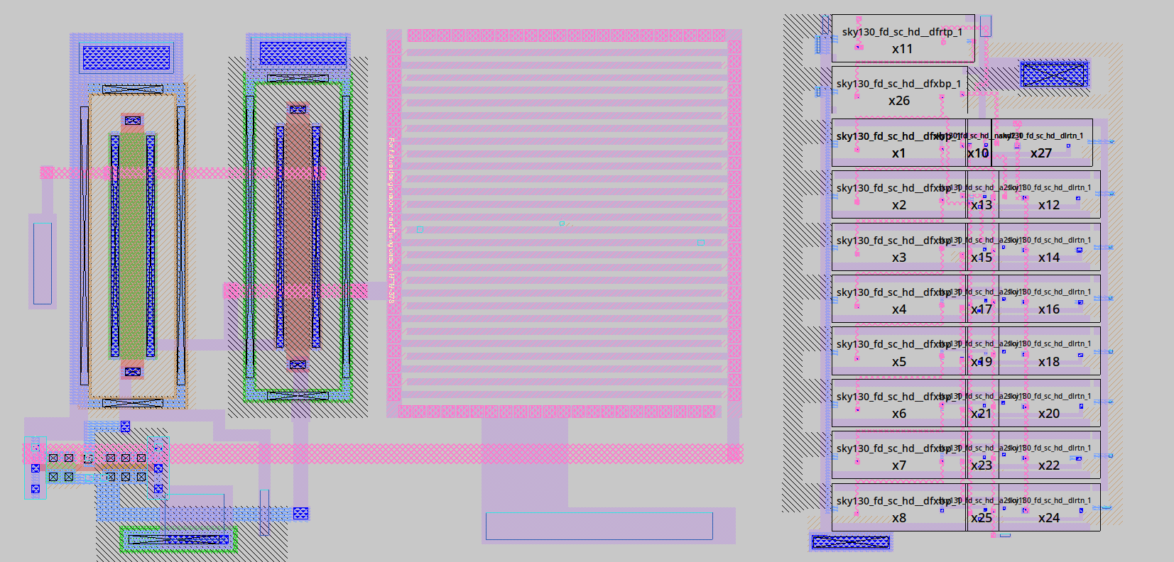
Layouts of the analog block were done using the magic layout software in a hierarchical manner. I leveraged standard cell blocks when possible, and laid out each subcomponent individually. On the left is a sample-and-hold register; on the right is the approximation register and logic.

The goal of this project was to develop a simple proof-of concept micrcontroller using the open source SKY130A PDK and an open source schematic and layout toolchain. The microcontroller consisted of an analog block (8-bit SAR ADC) and a digital block (4-bit CPU, SPI driver and small built-in RAM). The design process encompassed the whole stack of mixed-signal and digital ASIC design:
- For the analog block, I drew up a schematic using xschem, with four subcomponents - a sample-and-hold, a comparator, a register, and an R2R DAC. Each part was equipped with a simple testbench, and so was the full ADC. Level shifters had to be employed, since the logic level was 1.8V but VDDA was 3.3V.
- NGSpice was used for netlisting and simulation, generating analog waveform plots of the circuit's operation. This let me iteratively refine my design to dial in timing constraints with the approximation register and comparator.
- Magic was used to layout the analog block by hand. I laid out each subcomponent individually, defining its port locations and size, then stitched them together hierarchically to finalize the ADC as a whole.
- Netgen was used to perform LVS and DRC checks on the design, then extract layout parasitic capacitances and resistances. These were worked back into a second level of SPICE simulation.
- The CPU was designed with a simple instruction set with an 8-bit PC and a 4-bit accumulator, a set of control latches, an ALU capable of addition and bitwise logic, and an SPI driver for external program storage (flash or EEPROM). The instruction set included opcodes to load and store control registers to control peripherals like the ADC.
- The digital block was designed fully in verilog, using a SKY130 DFFRAM macro for built-in storage. iverilog and GTKWave were used to simulate the digital subcomponents and the CPU entirely digitally.
- I used the librelane toolchain to perform automated place-and-route on the digital design, including the DFFRAM macro, generating both layout files and SPICE files using the standard cell libraries in the PDK. I simulated these components using NGSpice as well, and ran DRC and LVS to validate the PnR.
- Finally, the digital and analog blocks were stitched together using magic and validation (DRC, LVS, parasitic extraction) was performed a final time to ensure the design was OK in its totality.

You may also like

Back to Top